This is a practical guide to Surface Science for researchers working in the Semiconductors Industry.
In this all-new guide you’ll learn all about:
Let’s dive right in.

Semiconductor manufacturers face the constant challenge of maximizing performance and refining processes. Often underestimated, surface properties play a crucial role in optimizing these performances. By measuring these properties, we gain valuable insights into material properties, processes, and device performance, ultimately leading to:
We use the following surface properties to understand the behavior of Semiconductors products and improve their quality.
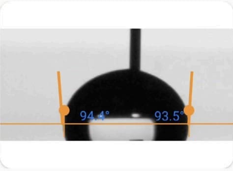
Sample Image taken from Droplet Lab Tensiometer.
Young – Laplace Method
Polynomial Method
Ideally, when we place a drop on a solid surface, a unique angle exists between the liquid and the solid surface. We can calculate the value of this ideal contact angle (the so-called Young’s contact angle) using Young’s equation. In practice, due to surface geometry, roughness, heterogeneity, contamination, and deformation, the contact angle value on a surface is not necessarily a single consistent value but rather falls within a range. The upper and lower limits of this range are known as the advancing and receding contact angles, respectively. The values of advancing and receding contact angles for a solid surface are highly sensitive to many parameters, such as temperature, humidity, homogeneity, and minor contamination of the surface and liquid. For example, the advancing and receding contact angles of a surface can differ at different locations.
Practical surfaces and coatings naturally show contact angle hysteresis, indicating a range of equilibrium values. When we measure static contact angles, we get a single value within this range. Solely relying on static measurements poses problems, like poor repeatability and incomplete surface assessment regarding adhesion, cleanliness, roughness, and homogeneity.
In practical applications, we need to understand how easily a liquid spreads (advancing angle) and how easily it is removed (receding angle), such as in painting and cleaning. Measuring advancing and receding angles offers a holistic view of liquid-solid interaction, unlike static measurements, which yield an arbitrary value within the range.
This insight is crucial for real-world surfaces with variations, roughness, and dynamics, aiding industries like cosmetics, materials science, and biotechnology in designing effective surfaces and optimizing processes.
Learn how Contact Angle measurement is done on our Tensiometer
For a more complete understanding of Contact Angle measurement, read our Contact Angle measurement: The Definitive Guide
These reference measurements show how deionized water wets four standard substrates measured with the Droplet Lab Dropometer. Use them as visual and numerical benchmarks when you're checking your own sample preparation, treatments, and chemistry.
Full contact angle and surface energy datasets (including additional liquids and statistics) are available on our dataset hub.
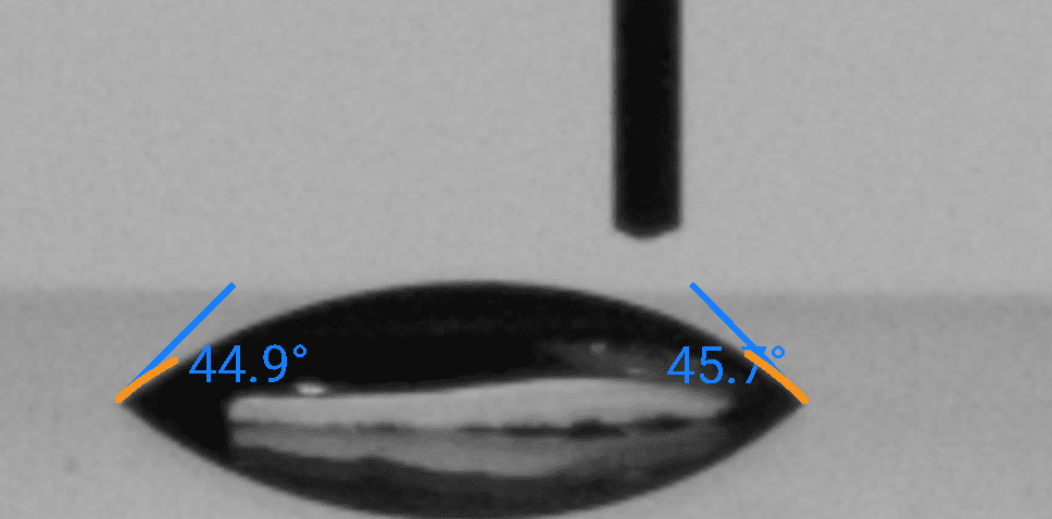
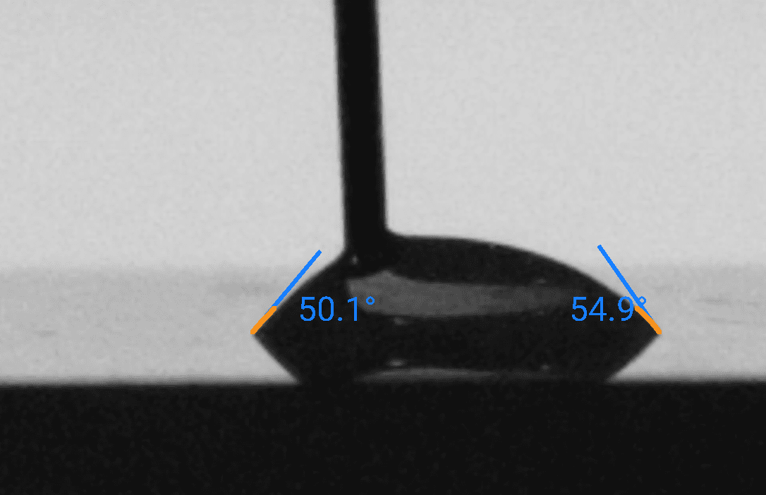
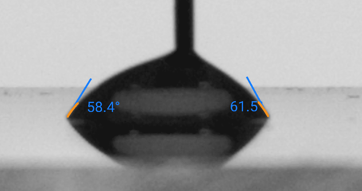
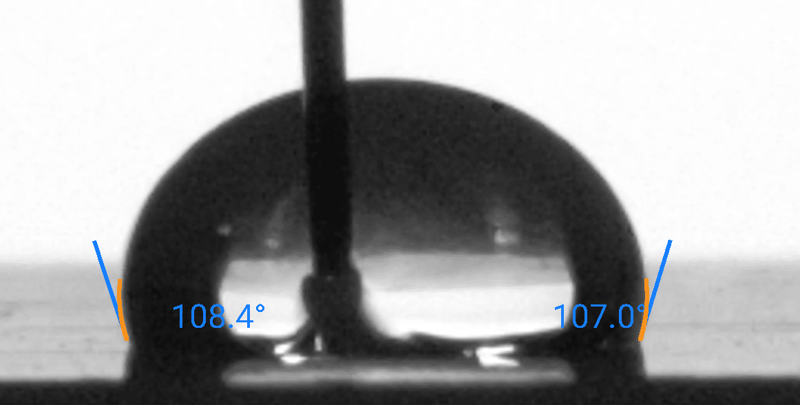
The droplet images above are taken from the same benchmark series as our open dataset. For each substrate and probe liquid we report:
● Advancing and receding contact angles (and hysteresis)
● Derived surface energy (SFE) values based on multi-liquid measurements
● Measurement conditions, uncertainties, and sample preparation details
Comparing your own droplet shapes and angles against these references is a fast way to spot contamination, treatment drift, or unexpected changes in wettability.
Measurements were performed with the Droplet Lab Dropometer under controlled laboratory conditions. Treat these values as sanity checks and starting points for your own process targets, not as product specifications.
This property measures the force that acts on the surface of a liquid, aiming to minimize its surface area.
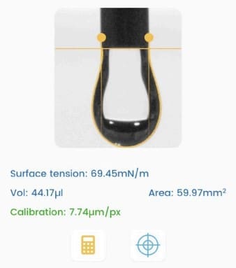
Sample Image taken from Droplet Lab Tensiometer
Dynamic Surface Tension
Dynamic surface tension differs from static surface tension, which refers to the surface energy per unit area (or force acting per unit length along the edge of a liquid surface).
Static surface tension characterizes the equilibrium state of the liquid interface, while dynamic surface tension accounts for the kinetics of changes at the interface. These changes could involve the presence of surfactants, additives, or variations in temperature, pressure, and composition at the interface.
When to use Dynamic Surface Tension Measurement
Dynamic surface tension is essential for processes that involve rapid changes at the liquid-gas or liquid-liquid interface, such as droplet and bubble formation, coalescence (change in surface area), the behavior of foams, and the drying of paints (change in composition, e.g., evaporation of solvent). It is measured by analyzing the shape of a hanging droplet over time.
Dynamic surface tension applies to various industries, including cosmetics, coatings, pharmaceuticals, paint, food and beverage, and industrial processes, where understanding and controlling the behavior of liquid interfaces is essential for product quality and process efficiency.
Learn how Surface Tension measurement is done on our Tensiometer
For a more complete understanding of Surface Energy measurement, read our Surface Tension measurement: The Definitive Guide
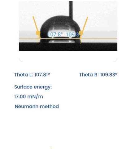
Sample Image taken from Droplet Lab Tensiometer
Learn how Surface Energy measurement is done on our Tensiometer
For a more complete understanding of Surface Energy measurement, read our Surface Energy measurement: The Definitive Guide
For benchmark contact angle and surface energy values on glass, nylon, PMMA, and Teflon, see the Open Benchmark Data panel above or visit our Dataset Hub for full CSV downloads.
The sliding angle measures the angle at which a liquid film slides over a solid surface. It is commonly employed to assess the slip resistance of a surface.
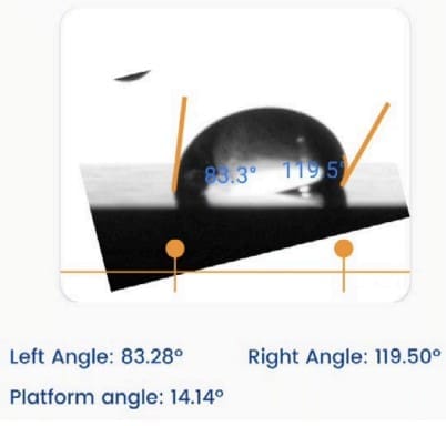
Sample Image taken from Droplet Lab Tensiometer
Learn how Sliding Angle measurement is done on our Tensiometer
For a more complete understanding of Sliding Angle measurement, read our Sliding Angle Measurement: The Definitive Guide
Within the Semiconductors industry, several case studies exemplify the advantages of conducting surface property measurements.
In photolithography, meticulous pattern creation is key to manufacturing complex semiconductor devices. This process relies heavily on the delicate interplay between the photoresist and the substrate. Photoresist adhesion to the substrate acts as a linchpin, directly determining the sharpness and precision of the resulting patterns. To achieve optimal results, manufacturers delve into the surface science of these properties. By examining the substrate's surface energy and analyzing the contact angle exhibited by the photoresist, they gain valuable insights to fine-tune adjustments.
This refining process enhances adhesion properties, ultimately leading to a seamless pattern transfer. The benefits are manifold, including increased yields, sharper results, and a significant reduction in defects throughout the lithography process.
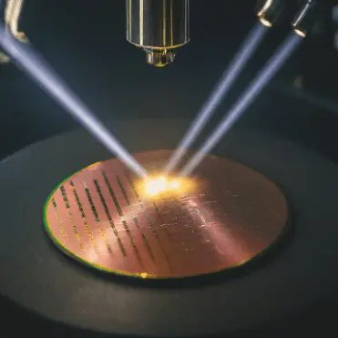
Chip packaging relies heavily on adhesives to securely bind the delicate semiconductor die to its protective casing. However, a major challenge arises from leftover adhesive residue, which can negatively impact device reliability.
To combat this issue, manufacturers meticulously measure and manage the sliding angle of the packaging material during application. This precise control ensures that the liquid adhesive smoothly glides away, leaving no unwanted residue behind. This optimization delivers two key benefits: firstly, it significantly reduces the risk of electrical shorts or unintended connections, and secondly, it effectively boosts the overall electrical performance of the device.

To achieve successful immersion lithography, meticulous management of the immersion fluid is crucial. A major failure point is the receding meniscus event, which leaves residual liquid behind on the wafer as a thin film or droplets. Ideally, the immersion fluid should be confined near the lens, allowing the wafer to scan smoothly during exposure.
For a semiconductor manufacturer, the meniscus failure mechanism remained a significant hurdle, hindering the successful implementation of immersion lithography. Recognizing the critical role of surface forces in drainage and pattern collapse during lithography, they sought a solution from a laboratory. The scientists, understanding the importance, developed a new fluid formulation with precisely tailored surface tension characteristics that facilitated proper liquid drainage, eliminating the meniscus issue.

If you are interested in implementing these or any other applications, please contact us.
In an industry where precision reigns supreme, how can Semiconductors manufacturers ensure their products withstand scrutiny? The answer lies in standards and guidelines: the compass that guides them through the complex maze of quality and performance.
Standard practice for estimating a solid’s total surface free energy and separating it into dispersive and polar components by measuring sessile‑drop contact angles of two probe liquids (one polar, one non‑polar) of known surface tension on the surface. It is intended as a quantitative, comparative surface‑readiness metric for wetting/adhesion process control within an approximate applicable range of ~20–60 mN/m.
Use fixed‑time contact angles plus calculated γ components to confirm surface cleaning/treatment/priming is within a validated “pass band” before committing to downstream trials.
Trend γs,polar/γs,dispersive and spot‑to‑spot variability to diagnose under‑treatment, contamination, non‑uniform treatment, or material/lot shifts.
This method provides an image‑backed, quantitative surface‑readiness signal but does not by itself guarantee adhesion or print performance. Any pass/fail gates must be calibrated per material family + treatment recipe + ink/adhesive system by correlating D7490 outputs to your downstream KPI.
We hope this guide showed you how to apply surface science in the Semiconductors industry.
Now we’d like to turn it over to you:
Feel free to leave a comment below—we’d love to hear from you.